

The Machine Worth $150 Million!!
ASML's upcoming generation's extreme ultraviolet lithography is the machine worth $150 million reaches historically unachievable accuracy, allowing chips to continue shrinking for years.
 Local BangaloreTeam
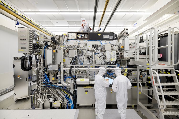
Engineers have begun building a crucial component for a machine that continues to keep the tech industry as we know it on track for at least another decade inside a large clean room in rural Connecticut. ASML, a Dutch firm, is building the machine. It has a monopoly in etching the tiniest nanoscopic details into microchips using light.
The machines play an important part in the chipmaking ecosystem, and they've been required to develop the latest, most sophisticated chips, such as those found in new iPhones and artificial intelligence systems. The company's latest EUV system, of which a portion is being developed in Wilton, Connecticut, will utilise a new technique to reduce the spectrum of light it uses, decreasing the size of features on the resultant chips and increasing their efficiency more than before. To put it in simple terms, the current generation of EUV devices is already a little insane.
They're about the size of a bus and cost $150 million each. There are 100,000 pieces in it, as well as 2 kilometers of wiring. The components must be transported using 40 freight containers, three cargo aircraft, and 20 vehicles. Only a few firms can finance the machines, and the vast majority of them go to the world's top three leading-edge chipmakers: TSMC, Taiwan's biggest foundry, as well as Samsung, South Korea, and Intel. “It's a truly innovative product, and a game-changer that will infuse fresh life into the business which will run for years.”
Launch
A massive piece of metal has been machined into a frame in Connecticut that will ultimately house a mask, or "reticle," that moves with nanoscale accuracy while reflecting a beam of severe ultraviolet light. The light bounces off multiple mirrors that have been sculpted and polished to carve details as small as a few hundred atoms into future computer chips. By the end of 2021, the completed component will be transported to Veldhoven, the Netherlands, and will be installed in the first prototype next-generation EUV machine by early 2022. The first chips created with the new technologies might be produced by Intel, which has stated that it would get the first batch by 2023.
The chips that the machine creates in the future years should be the quickest and most economical in history, with smaller features and tens of billions of components individually. ASML's newest EUV machine hopes to keep alive a concept that has come to embody growth not only in chip-making but in the computer sector and the economy as a whole. Gordon Moore, an electronics engineer and one of Intel's founders, authored an article for Electronics magazine's 35th-anniversary issue in 1965 that featured a comment that has since taken on a life of its own.
Moore's Law
Moore stated in the article that the quantity of information on a silicon chip had nearly quadrupled every year up to that point and that this tendency would continue. Moore changed his prediction a decade later to two years rather than one. In recent years, Moore's law has been called into question, while fresh manufacturing advances and chip design advancements have kept it on pace. EUV follows cutting-edge technology to lower the wavelength of light used in chip manufacturing, and it should help keep the streak going. The technology will be critical in the development of increasingly sophisticated smartphones and cloud computers, as well as in important new technology fields.
“The death of Moore's law has been grossly inflated. Midst the latest chip scarcity, triggered by the pandemic's financial shockwaves, ASML's products have now become central to a geopolitical tussle between the US and China, with Washington making blocking China's access to the machines top importance. The US government has successfully persuaded the Dutch not to provide the necessary export permits for the equipment to be sent to China, and ASML claims to have transported none to the nation. “A lot of it comes down to years and years of fiddling and trying, and getting access to that is really tough. Each component of a EUV machine is incredibly complex and specialised.
Manufacturing microchips already necessitates some of the world's most complex engineering. A chip begins as a cylindrical piece of crystalline silicon that is cut into thin wafers that are then covered with layers of light-sensitive material and subjected to structured light repeatedly. Chemical etching removes the portions of silicon that were not exposed to light, revealing the chip's fine features. After that, each wafer is broken up into a large number of individual chips.
The engineering issues, on the other hand, have taken decades to solve. Generating EUV light is a significant challenge itself. To create high-intensity light, ASML's approach requires focusing high-power lasers onto tin droplets 50,000 times per second. Because EUV frequencies are absorbed by lenses, the system relies on highly accurate mirrors covered with specific materials. TSMC, whose clients include Apple, Nvidia, and Intel, is the most well-known business employing EUV today. Intel was late to implement EUV and as a result lagged behind its competitors, prompting the company's recent decision to outsource some of its manufacturing to TSMC. ASML does not appear to believe that progress made on its devices would slow.